
FPGA and digital design
MIPS 16-bit Pipelined CPU
A five-stage MIPS-style 16-bit CPU in VHDL with hardware hazard control and a simple program-loading BIOS.
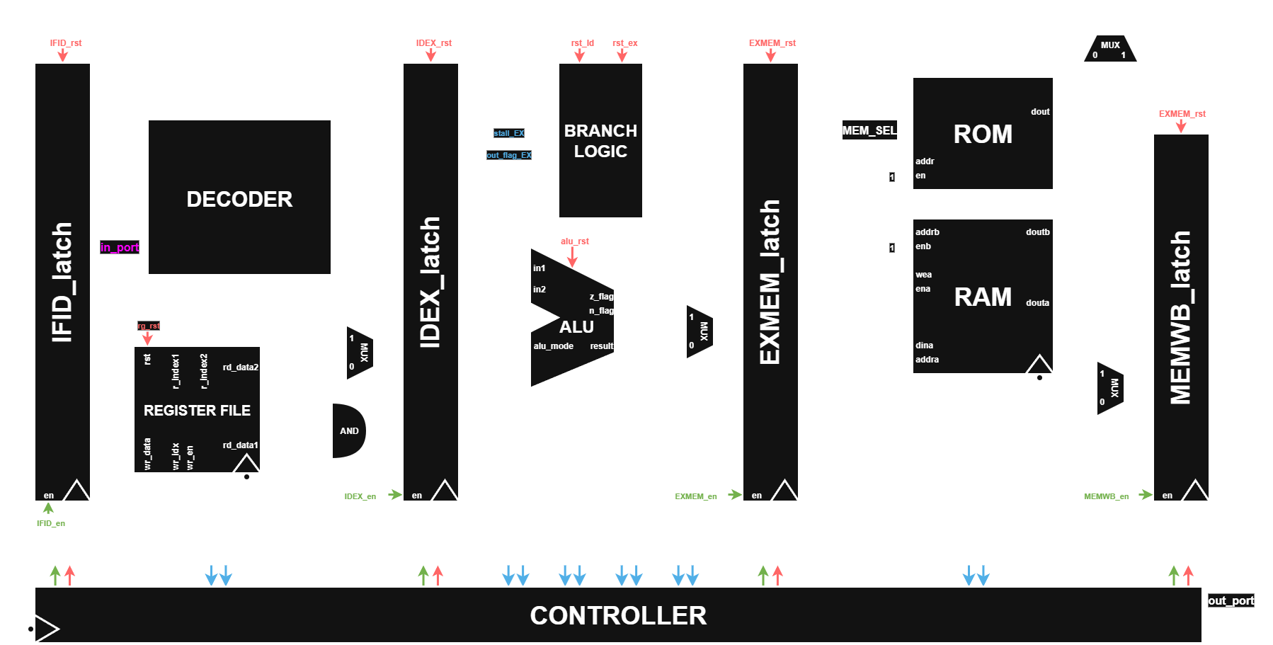
Overview
Hazard516 is a compact 16-bit RISC processor implemented in VHDL for FPGA hardware. Its five pipeline stages—IF, ID, EX, MEM, and WB—execute a course-defined instruction set with ALU, branch, memory, immediate, and I/O formats.
The design includes a BIOS in ROM that receives a program from an STM32 companion over I/O, writes it to RAM, and transfers execution to the loaded code.
Problem and context
Pipelining improves instruction throughput but introduces dependencies between instructions that are simultaneously in flight. The core needed to manage read-after-write hazards and taken branches in hardware rather than relying on programmer-inserted no-operations.
The complete FPGA demonstration also required a usable memory map and a path for loading programs without rebuilding the bitstream.
Technical approach
Synchronous IF/ID, ID/EX, EX/MEM, and MEM/WB latches separate the datapath. Decode selects register operands, immediate forms, ALU control, memory operations, branches, and IN/OUT behavior.
A pending-writeback bitmap tracks registers with in-flight writes. Decode stalls on a matching source, holds IF/ID, and injects a bubble into ID/EX; taken branches flush the younger pipeline stages.
Key engineering details
Instruction flow
The execution stage handles arithmetic, flags, effective addresses, and relative or register-based branches before results pass through memory and writeback.
Hazard controller
An eight-bit pending-writeback map detects RAW dependencies, inserts a single bubble, and clears entries when register writeback completes.
Memory and boot
ROM occupies 0x0000–0x03FF and RAM occupies 0x0400–0x07FF. The BIOS uses IN and OUT ports to load a user program before jumping to RAM.
Verification
VHDL testbenches cover the ALU, register file, and hazard-processing logic, while the integrated design targets a Basys 3 FPGA.
Results and outcomes
The bootloader runs on hardware and exercises the external I/O path. Pipeline latching, RAW stalls, bubble insertion, and taken-branch flushing are implemented without programmer-scheduled NOPs.
The project documentation also records an unresolved address-translation bug affecting LOAD and STORE when executing programs from RAM. Stack instructions, branch prediction, and timing-closure results are outside the implemented scope.